
The fast development of synthetic intelligence (AI) continues to revolutionize numerous sectors, extending past the tech business and permeating healthcare, finance, manufacturing, and even training. As these improvements surge ahead, one vital facet driving this transformation is the necessity for enhanced computational energy. Standard AI frameworks primarily depend on graphical processing models (GPUs) for mannequin coaching. Nevertheless, GPUs include important challenges, significantly regarding processing effectivity and power consumption. The hunt for a strong and sustainable infrastructure for AI has led researchers to discover different options that promise enhancements in each efficiency and power effectivity.
A groundbreaking research printed within the IEEE Journal of Chosen Subjects in Quantum Electronics has launched a novel AI acceleration platform that makes use of photonic built-in circuits (PICs). This strategy guarantees superior scalability and power effectivity, considerably outpacing conventional GPU-based architectures. Spearheaded by Dr. Bassem Tossoun, a Senior Analysis Scientist at Hewlett Packard Labs, this analysis underscores the potential of PICs to revolutionize the way in which AI workloads are executed. The combination of III-V compound semiconductors inside these circuits permits for outstanding operational effectivity, setting the stage for a brand new period of AI {hardware}.
Photonic AI accelerators introduce optical neural networks (ONNs), which function on the pace of sunshine, drastically lowering power loss in comparison with typical digital distributed neural networks (DNNs). This shift from digital to optical processing represents a considerable leap within the processing capabilities of AI techniques, aligning with the calls for of more and more complicated AI functions. Dr. Tossoun highlighted this transition, mentioning the inherent benefits supplied by silicon photonics, which whereas simple to fabricate, have traditionally posed challenges for scaling complicated built-in circuits.
The revolutionary strategy employed by Tossoun and his workforce concerned a heterogeneous integration of silicon photonics together with III-V compound semiconductors. This fusion of applied sciences enhances the infrastructure’s capability to combine important parts—corresponding to lasers and optical amplifiers—thereby minimizing optical losses and bettering total system scalability. Such developments allow PICs to accommodate quite a few functionalities in a compact footprint, making them superb candidates for next-generation AI accelerators.
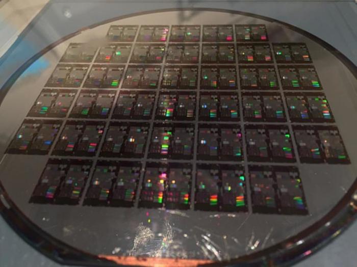
Fabrication of this state-of-the-art {hardware} started with silicon-on-insulator (SOI) wafers characterised by a 400 nm-thick silicon layer. The intricate course of concerned lithography, dry etching, and doping for setting up steel oxide semiconductor capacitor (MOSCAP) units and avalanche photodiodes (APDs). Subsequently, selective development methods have been employed to type layers important for optimum photoelectric efficiency within the PMD and combine III-V compounds onto the silicon substrate through die-to-wafer bonding. The ultimate shaping of this know-how noticed the addition of a skinny gate oxide layer and a strong dielectric layer, contributing to enhanced machine efficiency and stability.
Dr. Tossoun remarked, “The heterogeneous III/V-on-SOI platform presents the foundational parts important for advancing photonic and optoelectronic computing architectures tailor-made for AI/ML acceleration.” These architectures are extremely related for analog machine studying photonic accelerators that make the most of steady analog values, diverging considerably from typical digital approaches that are inclined to exacerbate power inefficiencies.
By attaining wafer-scale integration, the photonic platform permits the development of optical neural networks on a single chip, incorporating important parts corresponding to on-chip lasers, amplifiers, photodetectors, modulators, and part shifters. This in depth integration contributes to a dramatic enhance in power effectivity, with the brand new platform reportedly attaining a footprint-energy effectivity that’s 2.9 × 10² occasions higher than earlier photonic techniques and 1.4 × 10² occasions extra environment friendly than essentially the most refined digital electronics out there immediately.
This revolution in AI know-how, particularly by the lens of photonic circuits, hints at transformative potential throughout numerous functions. Addressing power prices and computational challenges will empower knowledge facilities to deal with an inflow of AI workloads, in the end resulting in enhanced capabilities in fixing complicated optimization issues—a necessity in immediately’s data-driven panorama. The longer term implications of this analysis stretch far and extensive, indicating a shift in the direction of a extra sustainable, environment friendly, and high-performance computational paradigm for AI functions.
The emergence of those photonic built-in circuits heralds a brand new chapter in AI {hardware} that isn’t merely an enhancement however a whole redefinition of what’s potential in machine studying and synthetic intelligence. As these technological developments attain maturation, industries can anticipate a big transformation of their operational capabilities, resulting in extra resilient and complex AI-driven options.
The promise of PICs extends past mere effectivity; it encapsulates a imaginative and prescient of a future the place AI computations can happen with minimal useful resource expenditure whereas maximizing efficiency outputs. This newly developed platform paves the way in which for strong, energy-efficient AI {hardware}, making certain that technological development stays each sustainable and accountable in an ever-evolving digital panorama.
As researchers and engineers proceed to refine these photonic approaches, the boundaries between algorithmic skills and {hardware} limitations will more and more diminish. This synergy won’t solely improve AI’s present functions however can even unlock totally new potentialities—enabling machines to be taught and adapt at unprecedented charges, essentially remodeling our relationship with know-how.
In abstract, the work executed by Tossoun and his workforce represents a paradigm shift in how technological developments can align with the long run power and computational wants of AI. This innovation is crucial for fostering a thriving setting for AI growth, the place effectivity meets scalability and efficiency, laying the groundwork for a brand new era of clever techniques.
Topic of Analysis: Photonic built-in circuits for AI acceleration
Article Title: Giant-Scale Built-in Photonic Gadget Platform for Vitality-Environment friendly AI/ML Accelerators
Information Publication Date: 9-Jan-2025
Net References: IEEE Journal of Chosen Subjects in Quantum Electronics
References: Tossoun, B., et al. (2025). Giant-Scale Built-in Photonic Gadget Platform for Vitality-Environment friendly AI/ML Accelerators. IEEE Journal of Chosen Subjects in Quantum Electronics.
Picture Credit: Bassem Tossoun from IEEE JSTQE
Key phrases
Tags: developments in AI computational poweralternatives to GPU for AIDr. Bassem Tossoun’s analysis contributionsenergy-efficient AI computingIEEE analysis on AI hardwareIII-V compound semiconductors in photonicsoptical neural networks technologyphotonic built-in circuits in AIrevolutionizing AI with photonicsscalable AI acceleration platformssilicon photonics for AI hardwaresustainable AI infrastructure